(Hong Kong)

Product Summary
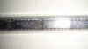
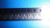
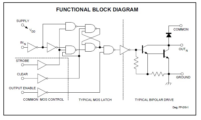
The UCN5801A latched-input BiMOS IC merges high-current, high-voltage outputs with CMOS logic. The CMOS input section consists of 4 or 8 data (‘D’ type) latches with associated common CLEAR, STROBE, and OUTPUT ENABLE circuitry. The power outputs are bipolar npn Darlingtons. This merged technology of the UCN5801A provides versatile, flexible interface. The BiMOS power interface IC UCN5801A greatly benefits the simplification of computer or microprocessor I/O. The device supersedes the original BiMOS latched-input driver ICs (UCN4400A and UCN4801A).
Parametrics
UCN5801A absolute maximum ratings: (1)Output Voltage, VCE: 50 V; (2)Supply Voltage, VDD: 15 V; (3)Input Voltage Range, VIN: -0.3 V to VDD + 0.3 V; (4)Continuous Collector Current, lC: 500 mA; (5)Package Power Dissipation, PD: See Graph; (6)Operating Temperature Range, TA: -20℃ to +85℃; (7)Storage Temperature Range, TS: -55℃ to +150℃.
Features
UCN5801A features: (1)To 4.4 MHz Data Input Rate; (2)High-Voltage, High-Current Outputs; (3)CMOS, NMOS, TTL Compatible Inputs; (4)Output Transient Protection; (5)Internal Pull-Down Resistors; (6)Low-Power CMOS Latches; (7)Automotive Capable.
Diagrams
 |
 UCN5800A |
Other |
|
Data Sheet |
Negotiable |
|
||||
|
UCN5804B |
Other |
|
Data Sheet |
Negotiable |
|
||||
|
UCN5810A |
Other |
|
Data Sheet |
Negotiable |
|
||||
|
UCN5810AF |
Other |
|
Data Sheet |
Negotiable |
|
||||
|
UCN5810EPF |
Other |
|
Data Sheet |
Negotiable |
|
||||
|
UCN5810LWF |
Other |
|
Data Sheet |
Negotiable |
|
||||